- 您现在的位置:买卖IC网 > Sheet目录1210 > DLP-HS-FPGA2 (DLP Design Inc)MODULE USB ADAPTER FOR FT2232H
�� �
�
�The� User� I/O� Block� controls� access� to� the� 63� user� I/O� pins� accessible� through� the� top-� and� bottom-�
�side� headers.� Every� one� of� these� pins� can� be� either� an� input� or� an� output.� The� User� I/O� Block� can�
�configure� these� pins� as� inputs� and� read� their� state,� or� as� outputs� and� drive� them� high� or� low.� (As� a�
�side� note,� 48� of� these� user� I/O� pins� can� be� configured� as� 24� differential� pairs,� 8� can� be� configured� as�
�global� clock� inputs� and� 6� can� be� configured� as� regional� clock� inputs.)�
�The� DDR2� SDRAM� interface� block� manages� the� memory’s� initialization,� the� refresh� cycle� and� the�
�read� and� write� access.� Read� and� write� access� is� available� in� 4-byte� bursts.� The� traces� between� the�
�DDR2� SDRAM� and� FPGA� are� matched� within� 10� mils� to� accommodate� reliable� data� transfer� at� 266�
�Mbit/s� (clocked� at� 133MHz).� The� interface� creates� and� aligns� the� Data� Strobes� (DQS)� based� on� an�
�external� feedback� trace� that� matches� two� times� the� trace� length� between� the� FPGA� and� the� DDR2�
�SDRAM.� The� Initialization,� Read� and� Write� commands� are� initiated� by� the� USB� interface� block� and�
�executed� by� the� DDR2� SDRAM� interface� block.�
�The� Heartbeat� Pulse� Generator� takes� the� internal� system� clock� and� divides� it� down� so� that� the�
�onboard� Heartbeat� LED� will� be� turned� on� and� off� for� a� duration� of� approximately� one-half� second.�
�The� Clock� Generator� Block� receives� the� 66-MHz� clock� and� produces� both� the� 133-MHz� clocks�
�required� to� run� the� DDR2� SDRAM� memory� device� and� the� 100-MHz� clock� for� the� remaining� internal�
�logic� in� the� FPGA.� It� also� handles� reset� and� lock� synchronization� between� internal� DCM� blocks.�
�The� design� occupies� the� following� FPGA� resources� on� the� DLP-HS-FPGA� module’s� XC3S200A:�
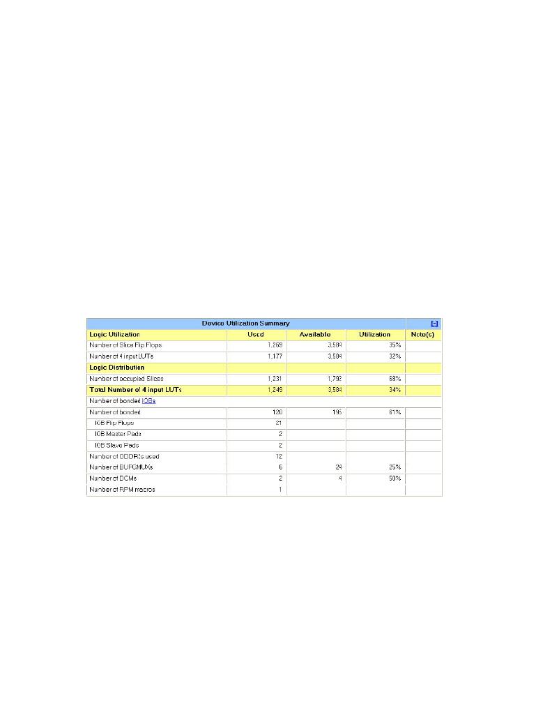
�The� design� occupies� the� following� FPGA� resources� on� the� DLP-HS-FPGA2� module’s� XC3S400A:�
�Rev.� 1.7� (May� 2011)�
�4�
�?� DLP� Design,� Inc.�
�发布紧急采购,3分钟左右您将得到回复。
相关PDF资料
DLP-IOR4
MODULE LATCHING-RELAY 4-CH
DLP-TEMP-G
MODULE DATA-ACQUISITION 3-CH
DLP-TXRX-G
MODULE USB-TO-TTL SRL UART CONV
DLP-USB1232H
MODULE USB-TO-UART/FIFO HS 18DIP
DLP-USB232M-G
MODULE USB-TO-TTL SRL UART CONV
DLP-USB232R
MODULE USB-TO-SRL UART 18-DIP
DLP-USB245M-G
MODULE USB-TO-TTL PARL FIFO CONV
DLP-USB245R
MODULE USB-TO-PARL FIFO 18-DIP
相关代理商/技术参数
DLP-HS-FPGA3
功能描述:可编程逻辑 IC 开发工具 USB-to-FPGA Development Module
RoHS:否 制造商:Altera Corporation 产品:Development Kits 类型:FPGA 工具用于评估:5CEFA7F3 接口类型: 工作电源电压:
DLP-HS-FPGA-A
功能描述:FPGA Embedded Module Spartan-3A, XC3S200A FT2232H 66MHz 32MB 制造商:dlp design inc. 系列:FPGA 零件状态:有效 模块/板类型:FPGA,USB ?? 核心处理器:Spartan-3A,XC3S200A 协处理器:FT2232H 速度:66MHz 闪存大小:- RAM 容量:32Mb 连接器类型:USB - B,引脚接头 大小/尺寸:3" x 1.2"(76.2mm x 30.5mm) 工作温度:0°C ~ 70°C 标准包装:1
DLP-IO14
功能描述:数据记录与采集 14-Channel Data-Acq Module
RoHS:否 制造商:Lantronix 描述/功能:Analog device server 显示器类型:None 电流额定值:
DLP-IO16
功能描述:界面模块 USB/Micro Dev Board
RoHS:否 制造商:4D Systems 产品:Serial Converters 通道/端口数量: 数据速率: 接口类型:USB, UART 工作电源电压:3.3 V, 5 V 最大工作温度:
DLP-IO20
功能描述:数据记录与采集 USB-BASED 20-CHANNEL DATA ACQUISITION MOD RoHS:否 制造商:Lantronix 描述/功能:Analog device server 显示器类型:None 电流额定值:
DLP-IO26
功能描述:开发板和工具包 - PIC / DSPIC USB/Micro Dev Board
RoHS:否 制造商:Microchip Technology 产品:Starter Kits 工具用于评估:chipKIT 核心:Uno32 接口类型: 工作电源电压:
DLP-IO8
功能描述:界面模块 USB-BASED 8-CHANL DATA ACQUSITION MODL
RoHS:否 制造商:4D Systems 产品:Serial Converters 通道/端口数量: 数据速率: 接口类型:USB, UART 工作电源电压:3.3 V, 5 V 最大工作温度:
DLP-IO8-G
功能描述:数据记录与采集 USB-BASED 8-CHANL DATA ACQUSITION MODL RoHS:否 制造商:Lantronix 描述/功能:Analog device server 显示器类型:None 电流额定值: